Silicon Valley's Next Big Leap: San Jose Optical Chip Facility Poised for Early 2026 Launch
Manufacturing
2025-04-14 12:30:15Content
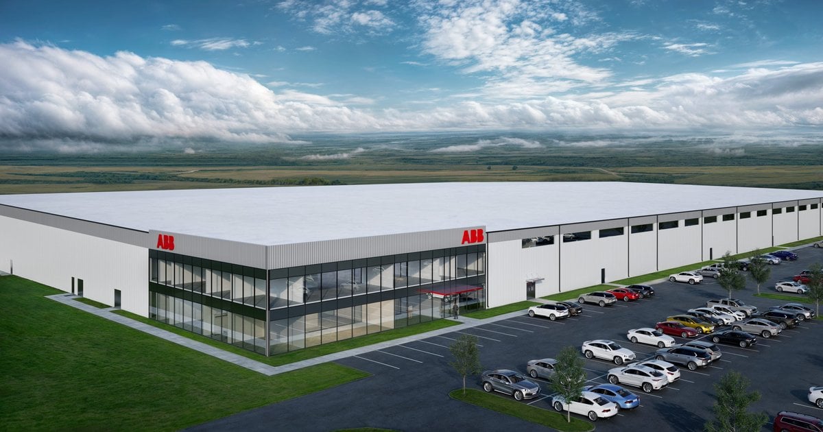
San Jose is poised to become a cutting-edge hub for photonics semiconductor technology, with a major new manufacturing facility set to launch initial operations in 2026. This state-of-the-art plant promises to be a game-changer in the semiconductor industry, bringing advanced photonic technology to the heart of Silicon Valley. The facility represents a significant investment in next-generation semiconductor manufacturing, potentially positioning San Jose at the forefront of innovative tech infrastructure. As the project moves forward, it is expected to create new job opportunities and reinforce the region's reputation as a global leader in technological innovation.
Silicon Valley's Photonics Revolution: A Groundbreaking Semiconductor Facility Emerges in San Jose
In the heart of Silicon Valley, a technological transformation is quietly taking shape, promising to redefine the semiconductor landscape with an unprecedented photonics manufacturing facility that could potentially reshape the region's technological ecosystem and economic trajectory.Pioneering the Future of Semiconductor Manufacturing in California's Tech Heartland
The Technological Landscape of Advanced Semiconductor Production
The semiconductor industry stands on the precipice of a monumental shift, with photonics technology representing a quantum leap in computational and communication capabilities. San Jose, long recognized as the global epicenter of technological innovation, is poised to become the birthplace of this revolutionary manufacturing initiative. Advanced photonics semiconductors represent a paradigm shift in electronic design, offering unprecedented performance metrics that traditional silicon-based technologies cannot match. Researchers and industry experts have long anticipated this moment, recognizing that photonics semiconductors could dramatically enhance signal processing speeds, reduce energy consumption, and enable more complex computational architectures. The proposed facility represents more than just a manufacturing plant; it symbolizes a strategic investment in cutting-edge technological infrastructure that could position the United States at the forefront of global semiconductor research and development.Economic and Technological Implications of the New Facility
The imminent establishment of this photonics semiconductor plant carries profound economic implications for San Jose and the broader Silicon Valley ecosystem. By attracting top-tier engineering talent and fostering an environment of technological innovation, the facility is expected to generate hundreds of high-skilled jobs and stimulate significant economic growth. Moreover, the plant's strategic location in San Jose provides immediate access to a robust network of research institutions, venture capital firms, and technology companies. This proximity creates a synergistic environment where technological breakthroughs can rapidly transition from conceptual designs to tangible manufacturing processes. The facility's potential to attract international attention could further solidify San Jose's reputation as a global technology hub.Technical Specifications and Manufacturing Capabilities
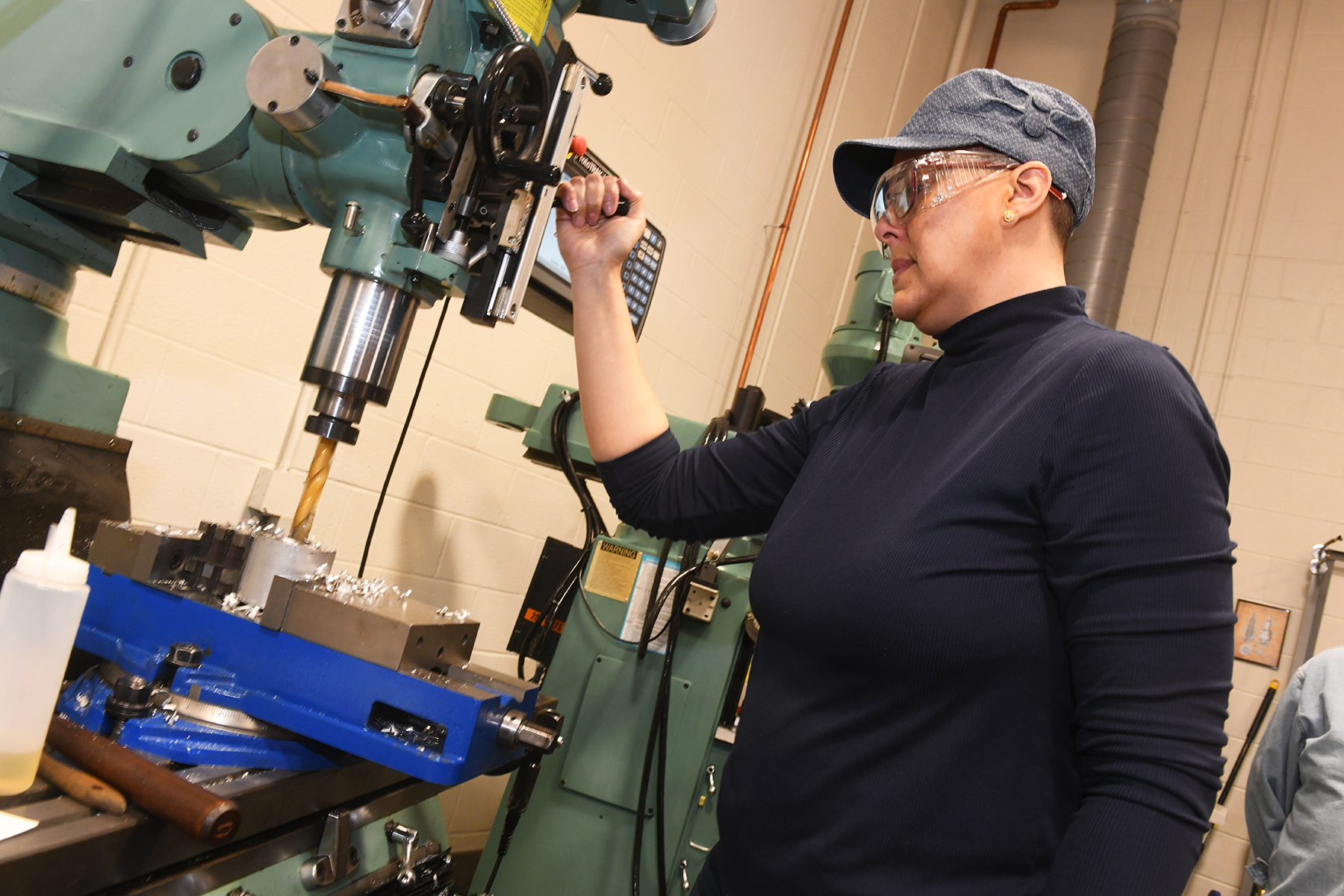
Preliminary reports suggest that the photonics semiconductor plant will incorporate state-of-the-art manufacturing technologies, including advanced lithography systems, precision optical alignment mechanisms, and sophisticated clean room environments. These technical capabilities will enable the production of semiconductor components with nanoscale precision, pushing the boundaries of what's currently possible in electronic miniaturization. The facility's projected initial operations in 2026 represent a carefully orchestrated timeline that allows for comprehensive testing, calibration, and incremental scaling of manufacturing capabilities. Industry analysts predict that the plant could potentially produce semiconductor components with performance characteristics that significantly outpace current market standards.Global Competitive Landscape and Strategic Positioning
In an era of increasing technological competition, this semiconductor facility represents a critical strategic asset for the United States. By investing in advanced photonics technologies, the project directly addresses the global semiconductor supply chain challenges that have emerged in recent years, potentially reducing dependence on international manufacturing networks. The plant's development signals a robust commitment to maintaining technological leadership, demonstrating that American innovation continues to drive global technological progress. Its establishment could inspire further investments in domestic semiconductor research and manufacturing, creating a ripple effect of technological advancement across multiple industries.RELATED NEWS
Manufacturing

"Enough is Enough": NY Manufacturer Demands Tariff Action to Protect American Industry
2025-04-21 19:50:07
Manufacturing
Investment Shift: Ruffer LLP Trims Stake in Tech Giant Taiwan Semiconductor
2025-03-09 11:55:24
Manufacturing
Breaking: Global Clinical Trial Supplies Market Set to Revolutionize Drug Development by 2029
2025-04-17 09:40:00