Breakthrough: Laser Holography Set to Transform Semiconductor Chip Production
Manufacturing
2025-04-12 00:12:00Content
Breakthrough Laser Technique Revolutionizes Semiconductor Chip Alignment with Unprecedented Precision
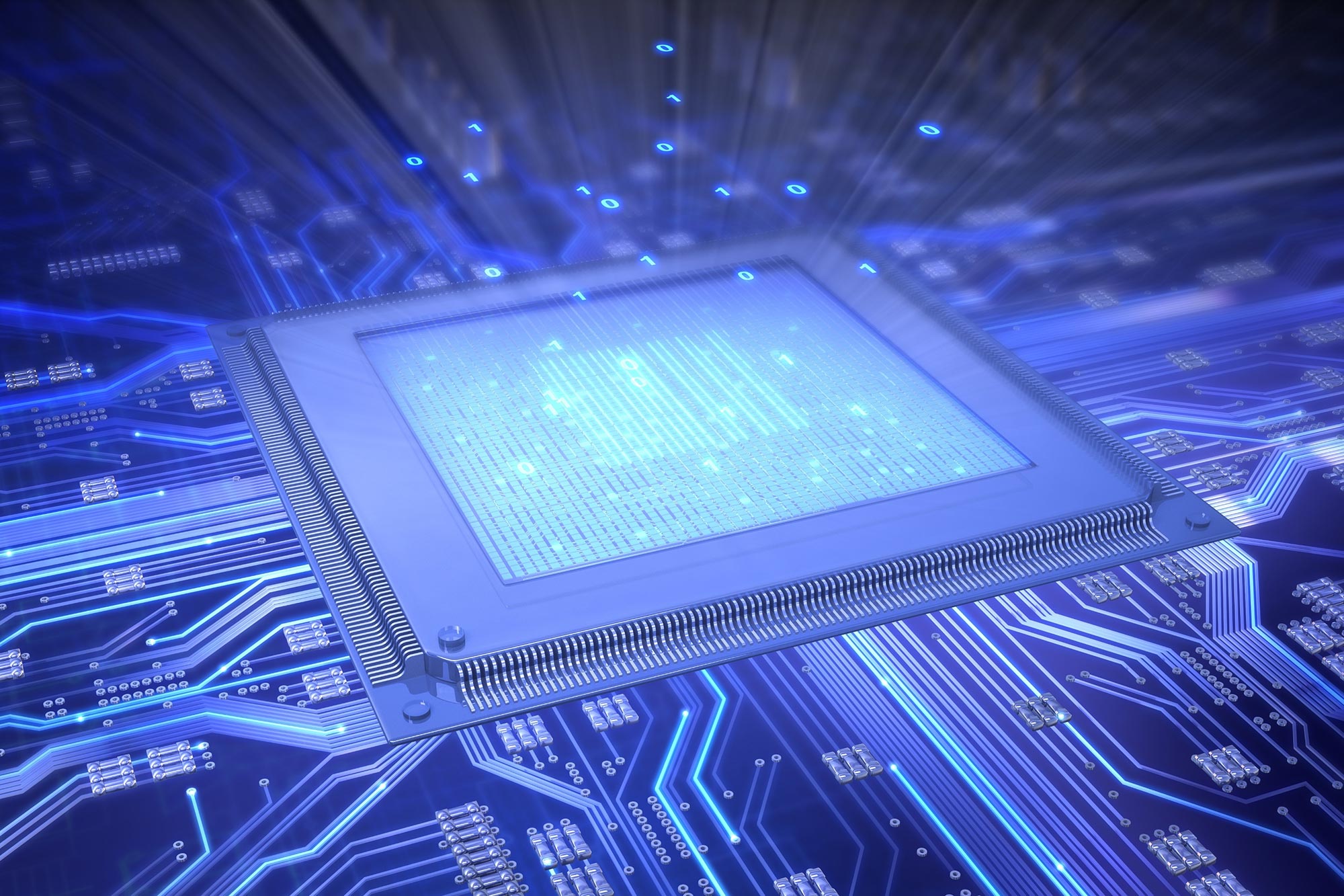
Scientists at the University of Massachusetts Amherst have unveiled a groundbreaking method for aligning 3D semiconductor chips that pushes the boundaries of technological precision. By employing an innovative approach using sophisticated lasers and intricate holographic techniques, researchers can now detect microscopic misalignments as incredibly small as 0.017 nanometers.
The cutting-edge technique involves projecting laser beams through carefully designed concentric metalenses patterned directly onto semiconductor chips. These precisely engineered metalenses create a sophisticated holographic mapping system that can identify even the most minute structural deviations with remarkable accuracy.
This revolutionary alignment method represents a significant leap forward in semiconductor manufacturing, promising to enhance the performance and reliability of complex electronic devices. By enabling such extraordinary levels of precision, the research could potentially transform how advanced microchips are designed, produced, and integrated into next-generation technologies.
Precision Unveiled: Revolutionizing Semiconductor Chip Alignment with Laser Holography
In the rapidly evolving landscape of technological innovation, researchers are constantly pushing the boundaries of what's possible in microelectronics. The intricate world of semiconductor manufacturing demands unprecedented levels of precision, where even the most microscopic misalignments can compromise the performance of cutting-edge electronic devices.Breakthrough Technology Promises Unprecedented Accuracy in Chip Manufacturing
The Quantum Leap in Semiconductor Precision
The realm of semiconductor engineering has long grappled with the challenge of achieving microscopic precision during chip fabrication. Traditional alignment methods have been limited by technological constraints, leaving manufacturers struggling to create increasingly complex electronic components. The groundbreaking research from the University of Massachusetts Amherst represents a quantum leap in addressing these fundamental challenges. Laser holography emerges as a transformative technology that fundamentally reimagines how semiconductor chips can be aligned with extraordinary accuracy. By leveraging advanced optical techniques, researchers have developed a method that transcends previous limitations, offering an unprecedented level of precision that was once considered impossible.Holographic Alignment: A Technological Marvel
The innovative approach utilizes sophisticated laser technology combined with intricate holographic patterning to detect and correct microscopic misalignments. What sets this method apart is its ability to identify deviations as minute as 0.017 nanometers - a scale so infinitesimal that it challenges conventional understanding of measurement. Imagine a technological process so precise that it can detect a misalignment smaller than a single atom. This is not science fiction, but a tangible breakthrough that could revolutionize semiconductor manufacturing. The researchers have effectively created a non-invasive, highly accurate alignment technique that promises to dramatically improve the quality and performance of electronic components.Implications for Future Technologies
The potential applications of this breakthrough extend far beyond current manufacturing processes. Advanced computing, quantum computing, artificial intelligence, and next-generation electronic devices could all benefit from this remarkable alignment technology. By ensuring unprecedented precision at the nanoscale, researchers are laying the groundwork for more powerful, efficient, and reliable electronic systems. Modern electronics demand increasingly complex and miniaturized components. The ability to align semiconductor chips with such extraordinary precision opens up new possibilities for designing smaller, faster, and more energy-efficient devices. From smartphones to supercomputers, every sector of technology stands to gain from this remarkable scientific advancement.Technical Complexity Decoded
At the heart of this innovation lies a complex interplay of optical physics and advanced engineering. The researchers developed concentric metalenses - intricate optical structures that can manipulate light with extraordinary precision. By carefully patterning these metalenses onto semiconductor chips and strategically directing laser beams, they created a measurement system capable of detecting the most minute structural variations. The technique represents a convergence of multiple scientific disciplines, demonstrating how interdisciplinary research can yield groundbreaking technological solutions. It's a testament to human ingenuity that we can now manipulate and measure matter at scales that were previously beyond our comprehension.Future Research and Development
While this breakthrough is remarkable, researchers emphasize that it represents just the beginning of a potentially transformative technological journey. Future iterations of this technique could further refine alignment processes, potentially reducing manufacturing costs and improving the reliability of electronic components. The scientific community is already buzzing with excitement about the potential applications and refinements of this laser holography approach. As research continues, we can anticipate even more sophisticated methods of achieving microscopic precision in semiconductor manufacturing.RELATED NEWS
Manufacturing
Gearing Up for Change: Inside the Transformation of North American Auto Supply Chains
2025-02-24 21:45:36
Manufacturing

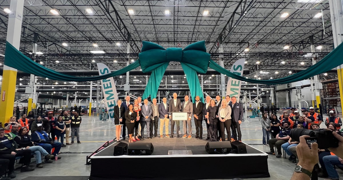
Chips on Home Soil: Nvidia's Bold Move to Bring AI Manufacturing Back to America
2025-04-14 13:06:21
Manufacturing

Cash Splash: How One Maryland City Is Luring Tech Nomads with a Jaw-Dropping Relocation Bonus
2025-02-25 01:41:58